- 您现在的位置:买卖IC网 > Sheet目录397 > BSS123_D87Z (Fairchild Semiconductor)MOSFET N-CH 100V 170MA SOT-23
�� �
�
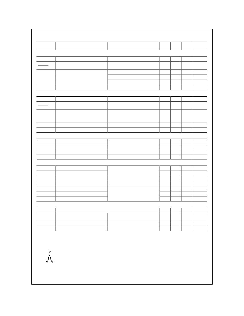
�Electrical� Characteristics�
�T� A� =� 25°C� unless� otherwise� noted�
�Symbol�
�Parameter�
�Test� Conditions�
�Min� Typ� Max�
�Units�
�Off� Characteristics�
�BV� DSS�
�Drain–Source� Breakdown� Voltage�
�V� GS� =� 0� V,�
�I� D� =� 250� μ� A�
�100�
�V�
�?� BV� DSS�
�?� T� J�
�Breakdown� Voltage� Temperature�
�Coefficient�
�I� D� =� 250� μ� A,Referenced� to� 25� °� C�
�97�
�mV/� °� C�
�I� DSS�
�Zero� Gate� Voltage� Drain� Current�
�V� DS� =� 100� V,�
�V� GS� =� 0� V�
�1�
�μ� A�
�V� DS� =� 100� V,V� GS� =� 0� V� T� J� =� 125� °� C�
�60�
�μ� A�
�V� DS� =� 20� V,�
�V� GS� =� 0� V�
�10�
�nA�
�I� GSS�
�Gate–Body� Leakage.�
�V� GS� =� ±� 20� V,�
�V� DS� =� 0� V�
�±� 50�
�nA�
�On� Characteristics�
�(Note� 2)�
�V� GS(th)�
�Gate� Threshold� Voltage�
�V� DS� =� V� GS� ,�
�I� D� =� 1� mA�
�0.8�
�1.7�
�2�
�V�
�?� V� GS(th)�
�?� T� J�
�Gate� Threshold� Voltage�
�Temperature� Coefficient�
�I� D� =� 1� mA,Referenced� to� 25� °� C�
�–2.7�
�mV/� °� C�
�R� DS(on)�
�Static� Drain–Source�
�V� GS� =� 10� V,�
�I� D� =� 0.17� A�
�1.2�
�6�
�?�
�On–Resistance�
�V� GS� =� 4.5� V,� I� D� =� 0.17� A�
�V� GS� = 10 V, I� D� = 0.17 A, T� J� = 125� °� C�
�1.3�
�2.2�
�10�
�12�
�I� D(on)�
�On–State� Drain� Current�
�V� GS� =� 10� V,�
�V� DS� =� 5� V�
�0.68�
�A�
�g� FS�
�Forward� Transconductance�
�V� DS� =� 10V,�
�I� D� =� 0.17� A�
�0.08�
�0.8�
�S�
�Dynamic� Characteristics�
�C� iss�
�C� oss�
�C� rss�
�Input� Capacitance�
�Output� Capacitance�
�Reverse� Transfer� Capacitance�
�V� DS� =� 25� V,�
�f� =� 1.0� MHz�
�V� GS� =� 0� V,�
�73�
�7�
�3.4�
�pF�
�pF�
�pF�
�R� G�
�Gate� Resistance�
�V� GS� =� 15� mV,� f� =� 1.0� MHz�
�2.2�
�?�
�Switching� Characteristics�
�(Note� 2)�
�t� d(on)�
�t� r�
�t� d(off)�
�t� f�
�Q� g�
�Q� gs�
�Turn–On� Delay� Time�
�Turn–On� Rise� Time�
�Turn–Off� Delay� Time�
�Turn–Off� Fall� Time�
�Total� Gate� Charge�
�Gate–Source� Charge�
�V� DD� =� 30� V,�
�V� GS� =� 10� V,�
�V� DS� =� 30� V,�
�V� GS� =� 10� V�
�I� D� =� 0.28� A,�
�R� GEN� =� 6� ?�
�I� D� =� 0.22� A,�
�1.7�
�9�
�17�
�2.4�
�1.8�
�0.2�
�3.4�
�18�
�31�
�5�
�2.5�
�ns�
�ns�
�ns�
�ns�
�nC�
�nC�
�Q� gd�
�Gate–Drain� Charge�
�0.3�
�nC�
�Drain–Source� Diode� Characteristics� and� Maximum� Ratings�
�I� S�
�Maximum Continuous Drain–Sourc� e� Diode� Forward� Current�
�0.17�
�A�
�V� SD�
�Drain–Source� Diode� Forward�
�V� GS� =� 0� V,�
�I� S� =� 0.34� A� (Note� 2)�
�0.8�
�1.3�
�V�
�Voltage�
�t� rr�
�Q� rr�
�Diode� Reverse� Recovery� Time�
�Diode� Reverse� Recovery� Charge�
�I� F� =� 0.17� A,�
�d� iF� /d� t� =� 100� A/μs�
�11�
�3�
�nS�
�nC�
�NOTE:�
�1.�
�R� θ� JA� is� the� sum� of� the� junction-to-case� and� case-to-ambient� thermal� resistance� where� the� case� thermal� reference� is� defined� as� the� solder� mounting� surface� of�
�the� drain� pins.� R� θ� JC� is� guaranteed� by� design� while� R� θ� CA� is� determined� by� the� user's� board� design.�
�a)� 350°C/W� when� mounted� on� a�
�minimum� pad..�
�Scale� 1� :� 1� on� letter� size� paper�
�2.�
�Pulse� Test:� Pulse� Width� ≤� 300� μ� s,� Duty� Cycle� ≤� 2.0%�
�BSS123� Rev� G(W)�
�发布紧急采购,3分钟左右您将得到回复。
相关PDF资料
BSS123TC
MOSFET N-CHAN 100V SOT23-3
BSS123W-7
MOSFET N-CH 100V 170MA SC70-3
BSS127S-7
MOSFET N CH 600V 50MA SOT23
BSS138_L99Z
MOSFET N-CH 50V 220MA SOT-23
BSS138DW-7
MOSFET DUAL N-CHAN 50V SC70-6
BSS138K
MOSFET N-CH 50V 220MA SOT-23-3
BSS138LT1
MOSFET N-CH 50V 200MA SOT-23
BSS138TC
MOSFET N-CHAN 50V SOT23-3
相关代理商/技术参数
BSS123_FAIRCHILD
制造商:FAIRCHILD 制造商全称:Fairchild Semiconductor 功能描述:
BSS123_NL
制造商:Fairchild Semiconductor Corporation 功能描述:Trans MOSFET N-CH 100V 0.17A 3-Pin SOT-23 T/R
BSS123_Q
功能描述:MOSFET SOT-23 N-CH LOGIC RoHS:否 制造商:STMicroelectronics 晶体管极性:N-Channel 汲极/源极击穿电压:650 V 闸/源击穿电压:25 V 漏极连续电流:130 A 电阻汲极/源极 RDS(导通):0.014 Ohms 配置:Single 最大工作温度: 安装风格:Through Hole 封装 / 箱体:Max247 封装:Tube
BSS123215
制造商:NXP Semiconductors 功能描述:MOSFET N CH 100V 150MA 3-SOT-23
BSS123-7
功能描述:MOSFET 100V 360mW RoHS:否 制造商:STMicroelectronics 晶体管极性:N-Channel 汲极/源极击穿电压:650 V 闸/源击穿电压:25 V 漏极连续电流:130 A 电阻汲极/源极 RDS(导通):0.014 Ohms 配置:Single 最大工作温度: 安装风格:Through Hole 封装 / 箱体:Max247 封装:Tube
BSS1237F
制造商: 功能描述: 制造商:undefined 功能描述:
BSS123-7-F
功能描述:MOSFET 100V 360mW RoHS:否 制造商:STMicroelectronics 晶体管极性:N-Channel 汲极/源极击穿电压:650 V 闸/源击穿电压:25 V 漏极连续电流:130 A 电阻汲极/源极 RDS(导通):0.014 Ohms 配置:Single 最大工作温度: 安装风格:Through Hole 封装 / 箱体:Max247 封装:Tube
BSS123-7-F-31
制造商:DIODES 功能描述:N-CHANNEL MOSFET / SOT-23 (LEAD FREE)